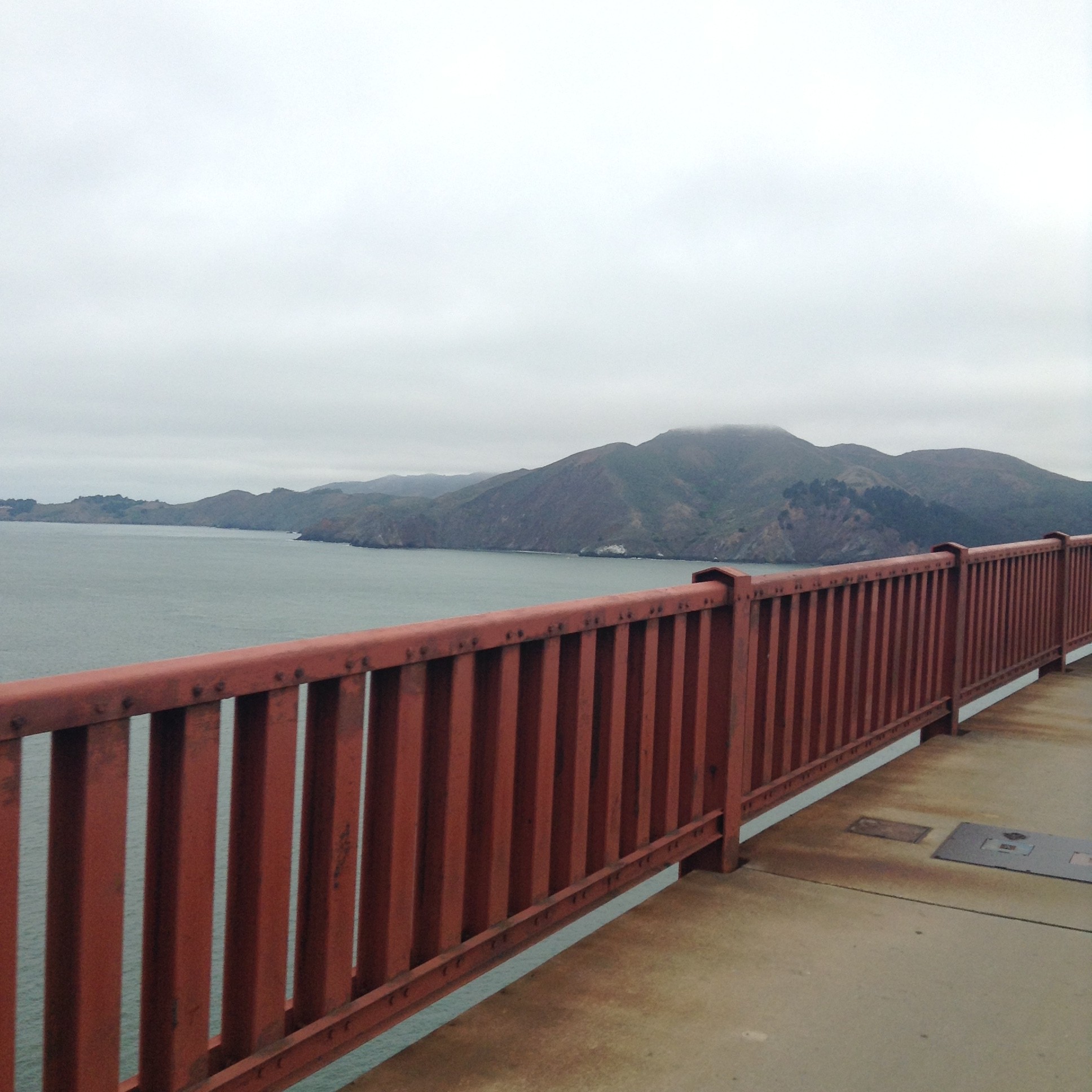
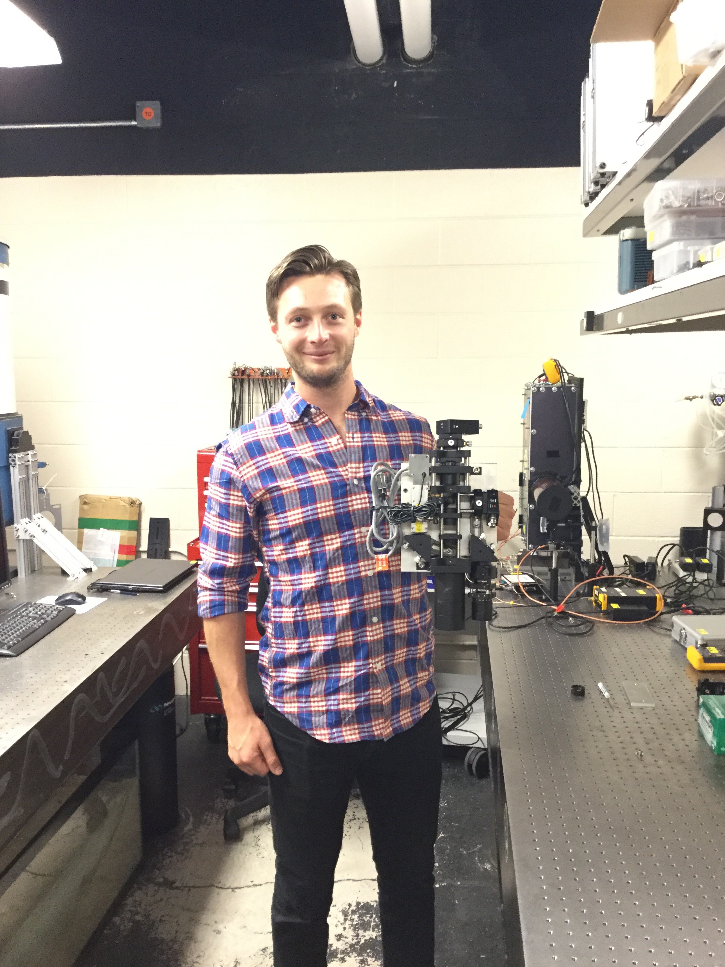
I’m back in San Francisco for Photonics West. A lot has changed since last time: I’m married, I graduated from my Ph.D., my wife and I moved to Canada, and I started a job as a process scientist at Excelitas Technologies Canada.
Through all of this I’ve worked to keep up my engagement with the optics and photonics professionals societies, and in particular with the SPIE, the international society for optics and photonics. I’ve started a second term as member of the SPIE Education committee and the Student and Early Career Professional Ad Hoc Committee. My attendance to Photonics West is supported by the SPIE and I’m grateful for the opportunity to keep contributing to the society’s missions in Education and for young professionals.
As a recent addition to the semiconductor manufacturing workforce, the program of my week looks at lot different to being a Ph.D. or postdoctoral researcher. SPIE offers courses that are pertinent to my field of work, which my employers value. I will be attending the following courses to develop my knowledge of the technical semiconductor sector in photonics, as well as skills on project management and product development.
- Semiconductor Photonic Device Fundamentals
- How to Develop Profitable Technology Products
- The Seven Habits of Highly Effective Project Managers
As always, a conference is a meeting and an excellent place for networking, learning about developments in the field of photonics, and finding people to collaborate on new and exciting projects. The first place you’ll be able to find me is on Sunday night from 9 pm at 21st Amendment Brewery for the SPIE Careers Lab meetup – see the Facebook event for more information. I’ll be around the conference at the technical sessions, the trade show and the special events. I’m also excited to be visiting Silicon Valley later in the week. More on that later. Follow this space for more details and if you’re in town, get in touch!